2
RF Device Data
Freescale Semiconductor
MRF7S21080HR3 MRF7S21080HSR3
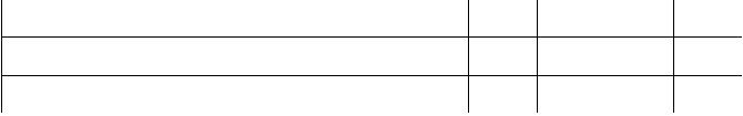
Table 3. ESD Protection Characteristics
Test Methodology
Class
Human Body Model (per JESD22--A114)
1C (Minimum)
Machine Model (per EIA/JESD22--A115)
A (Minimum)
Charge Device Model (per JESD22--C101)
IV (Minimum)
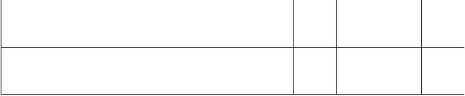
Table 4. Electrical Characteristics
(TA
=25°C unless otherwise noted)
Characteristic
Symbol
Min
Typ
Max
Unit
Off Characteristics
Zero Gate Voltage Drain Leakage Current
(VDS
=65Vdc,VGS
=0Vdc)
IDSS
?
?
10
μAdc
Zero Gate Voltage Drain Leakage Current
(VDS
=28Vdc,VGS
=0Vdc)
IDSS
?
?
1
μAdc
Gate--Source Leakage Current
(VGS
=5Vdc,VDS
=0Vdc)
IGSS
?
?
1
μAdc
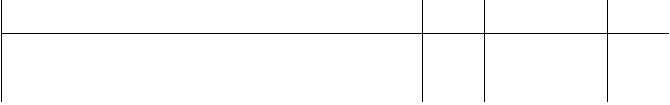
On Characteristics
Gate Threshold Voltage
(VDS
=10Vdc,ID
= 174
μAdc)
VGS(th)
1.5
2
3
Vdc
Gate Quiescent Voltage
(VDS
=28Vdc,ID
= 800 mAdc)
VGS(Q)
?
2.7
?
Vdc
Fixture Gate Quiescent Voltage
(1)
(VDD
=28Vdc,ID
= 800 mAdc, Measured in Functional Test)
VGG(Q)
4
5.5
7
Vdc
Drain--Source On--Voltage
(VGS
=10Vdc,ID
=1.74Adc)
VDS(on)
0.1
0.2
0.3
Vdc
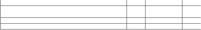
Dynamic Characteristics
(2)
Reverse Transfer Capacitance
(VDS
=28Vdc±
30 mV(rms)ac @ 1 MHz, VGS
=0Vdc)
Crss
?
0.64
?
pF
Output Capacitance
(VDS
=28Vdc±
30 mV(rms)ac @ 1 MHz, VGS
=0Vdc)
Coss
?
296
?
pF
Input Capacitance
(VDS
=28Vdc,VGS
=0Vdc±
30 mV(rms)ac @ 1 MHz)
Ciss
?
160
?
pF
Functional Tests
(In Freescale Test Fixture, 50 ohm system) VDD
=28Vdc,IDQ
= 800 mA, Pout
= 22 W Avg., f = 2167.5 MHz,
Single--Carrier W--CDMA, IQ Magnitude Clipping, PAR = 7.5 dB @ 0.01% Probability on CCDF. ACPR measured in 3.84 MHz Channel
Bandwidth @
±5MHzOffset.
Power Gain
Gps
16.5
18
19.5
dB
Drain Efficiency
ηD
30
32
?
%
Output Peak--to--Average Ratio @ 0.01% Probability on CCDF
PAR
5.7
6.5
?
dB
Adjacent Channel Power Ratio
ACPR
?
-- 3 8
-- 3 5
dBc
Input Return Loss
IRL
?
-- 1 6
-- 9
dB
1. VGG
=2xVGS(Q). Parameter measured on Freescale Test Fixture, due to resistive divider network on the board. Refer to Test Circuit
schematic.
2. Part internally matched both on input and output.
(continued)


发布紧急采购,3分钟左右您将得到回复。
相关PDF资料
MRF7S21110HSR5
MOSFET RF N-CH 33W NI-780S
MRF7S21150HSR5
MOSFET RF N-CH 150W NI780S
MRF7S21170HR5
IC MOSFET RF N-CHAN NI-880
MRF7S21210HSR5
MOSFET RF N-CH 63W NI-780S
MRF7S27130HSR5
MOSFET RF N-CH 23W NI-780S
MRF7S35015HSR5
MOSFET RF N-CH 15W NI-400S-240
MRF7S35120HSR5
MOSFET RF N-CH 120W NI-780S
MRF7S38010HSR5
MOSFET RF N-CH 2W 30V NI-400S
相关代理商/技术参数
MRF7S21110HR3
功能描述:射频MOSFET电源晶体管 HV7 33W WCDMA NH780H RoHS:否 制造商:Freescale Semiconductor 配置:Single 晶体管极性: 频率:1800 MHz to 2000 MHz 增益:27 dB 输出功率:100 W 汲极/源极击穿电压: 漏极连续电流: 闸/源击穿电压: 最大工作温度: 封装 / 箱体:NI-780-4 封装:Tray
MRF7S21110HR5
功能描述:射频MOSFET电源晶体管 HV7 33W WCDMA NH780H RoHS:否 制造商:Freescale Semiconductor 配置:Single 晶体管极性: 频率:1800 MHz to 2000 MHz 增益:27 dB 输出功率:100 W 汲极/源极击穿电压: 漏极连续电流: 闸/源击穿电压: 最大工作温度: 封装 / 箱体:NI-780-4 封装:Tray
MRF7S21110HS
制造商:Freescale Semiconductor 功能描述:
MRF7S21110HSR3
功能描述:射频MOSFET电源晶体管 HV7 33W WCDMA NI780HS RoHS:否 制造商:Freescale Semiconductor 配置:Single 晶体管极性: 频率:1800 MHz to 2000 MHz 增益:27 dB 输出功率:100 W 汲极/源极击穿电压: 漏极连续电流: 闸/源击穿电压: 最大工作温度: 封装 / 箱体:NI-780-4 封装:Tray
MRF7S21110HSR5
功能描述:射频MOSFET电源晶体管 HV7 33W WCDMA NI780HS RoHS:否 制造商:Freescale Semiconductor 配置:Single 晶体管极性: 频率:1800 MHz to 2000 MHz 增益:27 dB 输出功率:100 W 汲极/源极击穿电压: 漏极连续电流: 闸/源击穿电压: 最大工作温度: 封装 / 箱体:NI-780-4 封装:Tray
MRF7S21150HR3
功能描述:射频MOSFET电源晶体管 HV7 2.1GHZ 150W NI780HS RoHS:否 制造商:Freescale Semiconductor 配置:Single 晶体管极性: 频率:1800 MHz to 2000 MHz 增益:27 dB 输出功率:100 W 汲极/源极击穿电压: 漏极连续电流: 闸/源击穿电压: 最大工作温度: 封装 / 箱体:NI-780-4 封装:Tray
MRF7S21150HR3_09
制造商:FREESCALE 制造商全称:Freescale Semiconductor, Inc 功能描述:RF Power Field Effect Transistors N-Channel Enhancement-Mode Lateral MOSFETs
MRF7S21150HR5
功能描述:射频MOSFET电源晶体管 HV7 2.1GHZ 150W NI780HS RoHS:否 制造商:Freescale Semiconductor 配置:Single 晶体管极性: 频率:1800 MHz to 2000 MHz 增益:27 dB 输出功率:100 W 汲极/源极击穿电压: 漏极连续电流: 闸/源击穿电压: 最大工作温度: 封装 / 箱体:NI-780-4 封装:Tray
